2.0 - Architecture Overview
2.1 -
A computer components include a CPU (Central Processing Unit), a RAM (Random Access Memory), a storage device (SSD / HDD), input / output devices (screenm keyboard, mouse).
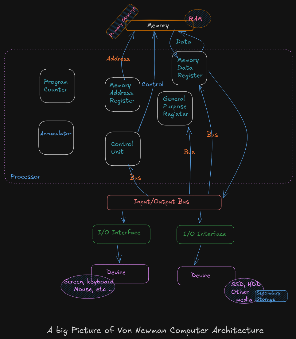
A Big Picture of Von Neumann Architecture
A CPU or processor is a computer brain that contains a Control Unit (CU), main memory, and Arithmetic Logic Unit (ALU) A CPU includes all circuitry required to process input, store data, and generate output. It also follows program instructions that tell it which information to process and how to process it.
-
CU (
Control Unit): It is responsible for how data moves throughout the system, for redirecting all input and output flow, and for fetching instruction code. -
ALU (
Arithmetic and Logic Unit) : It a part of CPU who handles all computations like addition, subtraction, and comparisons, with logical operations, arithmetic operations and bit shifting operation -
Register : It’s a sort of highly fast Computer memory that is used to accept, store, and transport data A Processor register is the term used to define the registers that CPU uses (General Purpose Register) .
-
Accumulator : It store the result of calculation that ALU makes.
-
Program Counter: The memory address of the next instruction (the instruction that will be executed next). This next address is passed from the Program Counter to the Memory Address Register.
-
Memory Address Register :
MARstores the memory address locations of those instructions that are either to be fetched from memory or to be stored in memory. -
Memory Data Register :
MDRstores the instructions that are fetched from memory or any information that is to be transferred to and stored in the memory. -
Current Instruction Register :
CIRstores the recently fetched instructions while they wait for execution. -
Instruction Buffer Register :
IBRis used to hold instructions that are not immediately executed.
Input / Output Devices
The program or the data is read into main memory (RAM) from the secondary storage (HDD, SSD)
If an result are evaluated by a computer and saved in it , you can present them to user via output devices.
-
Buses: Data is sent from one part of a computer to another via buses which connect all key internal components to the memory and CPU.
-
Control Bus: It receive control commands from
CPU, as well as status signals from other devices, and uses them to control and coordinate all of the computer’s actions. -
Address Bus: It communicates between memory and the processor data address (not the actual data)
-
Data Bus: It relays information between the memory unit, I/O devices, and the processor.
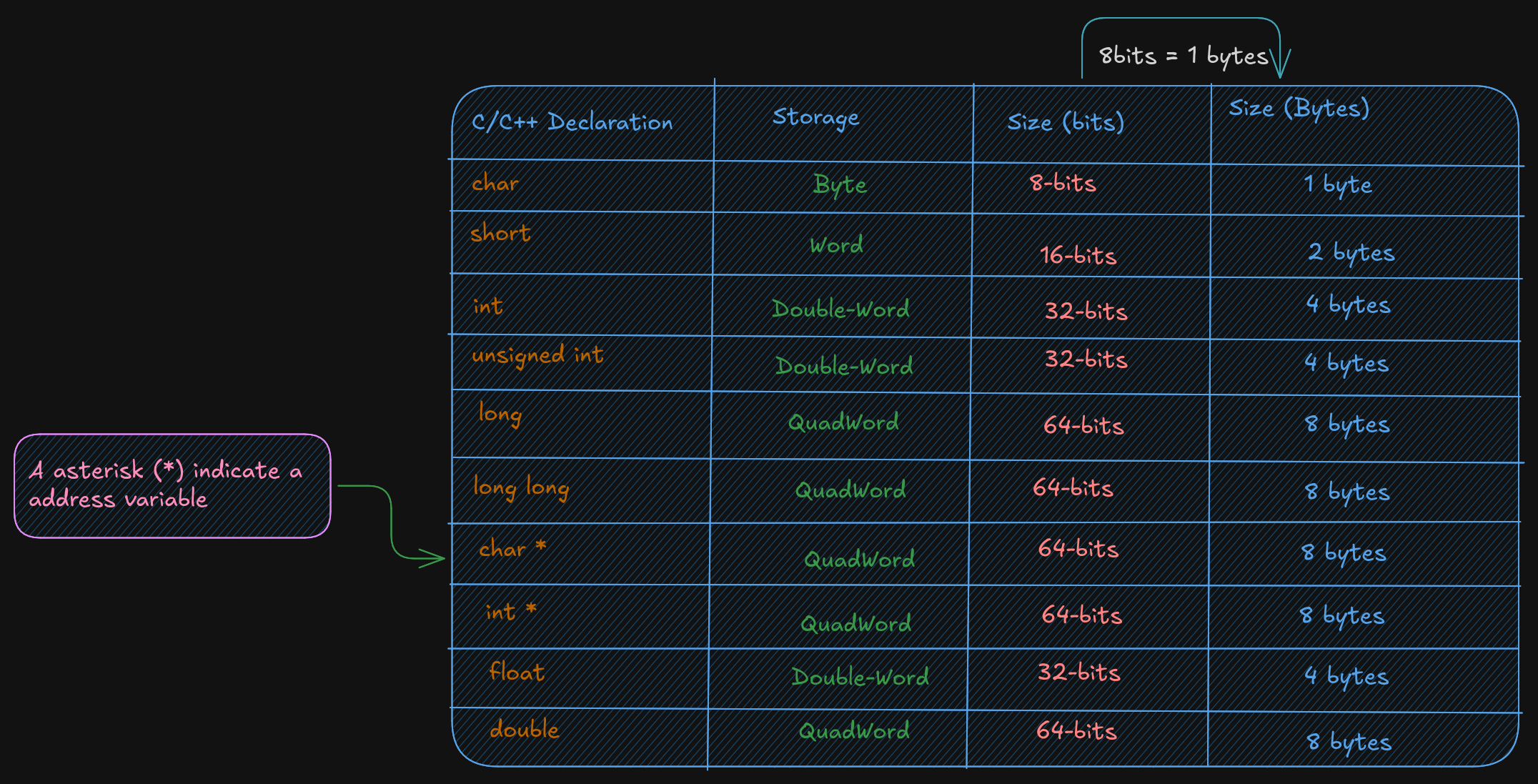
2.2 Data Storage Sizes
The x86-64 architecture supports a specific set of data storage size elements. The storage size are a direct correlation to variable declarations in high-level language (C, C++, Rust)
2.3 CPU Registers
A CPU Registers or just register, is a temporary storage or working
location built into the CPU itself (separate)
A 64-bit General Purpose Registers (GPRs) are in number of 60, they can
be used by all 64-bits or some portion or subset accessed.
When a data want to used a element with sizes less than 64-bits (32-bit, 16-bit, or 8-bit) a specific part of this less sized register can be accessed by using a different register name like described here :
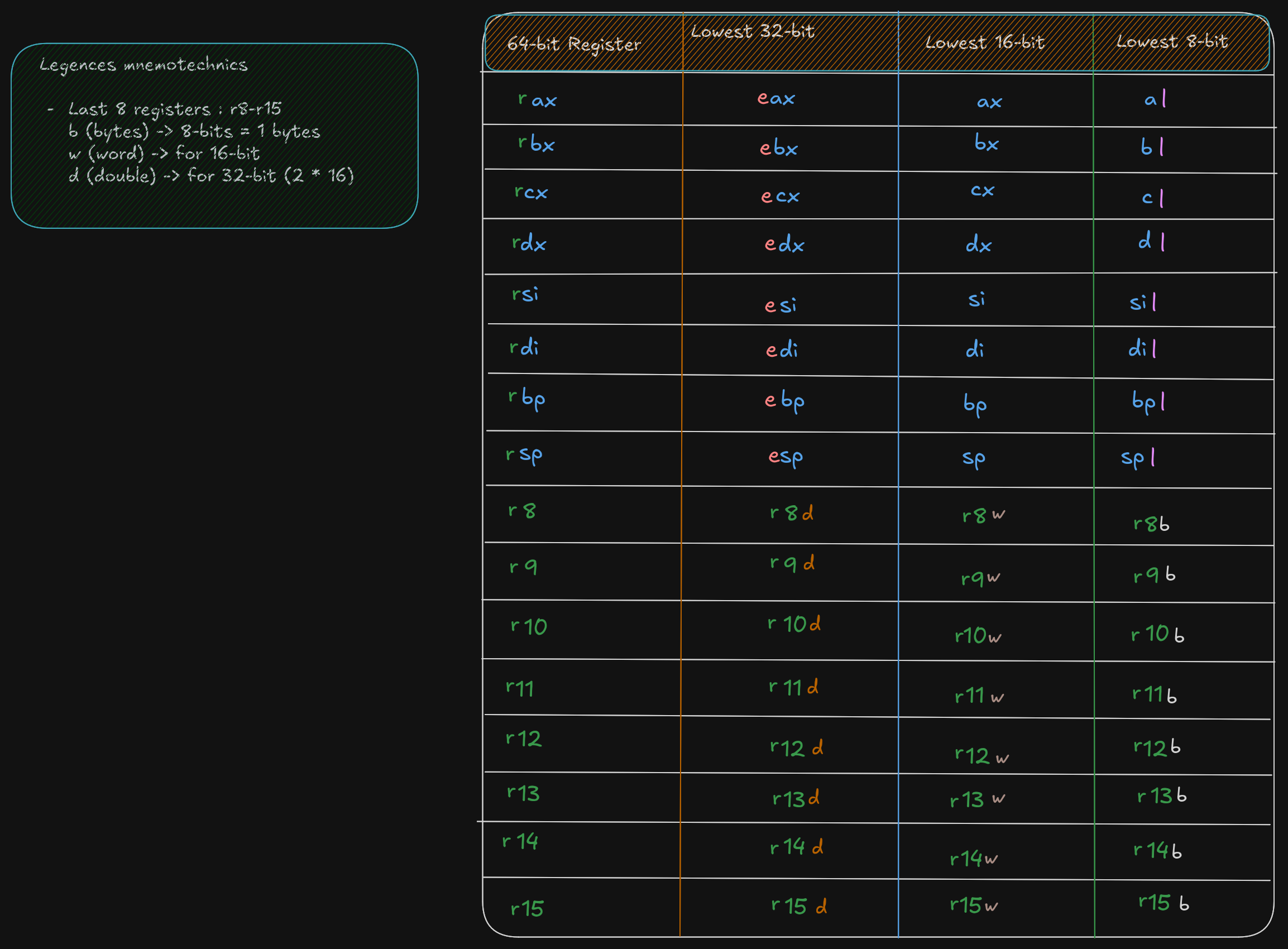
As show in the excalidrw diagram, the first 4 registers, rax, rbx, rcx,
rdx allow to accessed to 8-15 bits with the ah, bh, ch, and dh register names.
But ah is provided for legacy support.
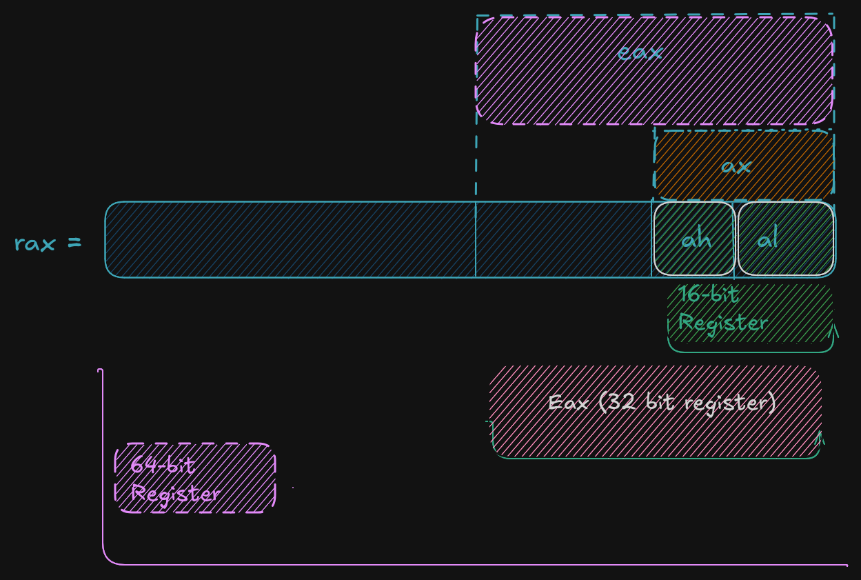
A register save value the used to affected to them in hex base. By exemple if:
rax = 50.000.000.000 	  # value set to rax in decimal base (10)
rax = 0000 000B A43B 7400 # the eax value is saved in hex base (16)

ax = 50.000 			  # if ax is set to 50.000 in base decimal (10)
ax = C350 				  # the ax calue is save in hex base 	(16)

rax = 0000 000B A43B C350 # each value is 1byte, the total do 16 byte, and each section separate by space do 16-bit
  # the total do 64-bit,  here the lower 16-bit ax of rax is set the upper 48-bits are unaffected
  # Note the change of ax to 7400 (16) to C350 (16)

al = 50					  # al register is set to 50 (10), who is 32 (16) in hex
rax = 0000 000B A43B C332 # when the lower 8-bit al portion of the 64-bit is set the 56-bits are unaffected
For 32-bit register operations, the upper 32-bit (first 32-bit from left to right) is set cleared (set to 0)
RSP (Register Stack Pointer)
A rsp is a register who is not used for data or other uses but it used to point to the top of the stack.
RBP (Register Base Pointer)
A rbp is used as a base pointer during functions calls, it her only functions.
RIP (Register Instruction Pointer)
A rip is a special register used by CPU ro point to the next instruction to be executed.
So if rip points to the next instruction means that in debugger the rip point to a instruction who is not
already executed.
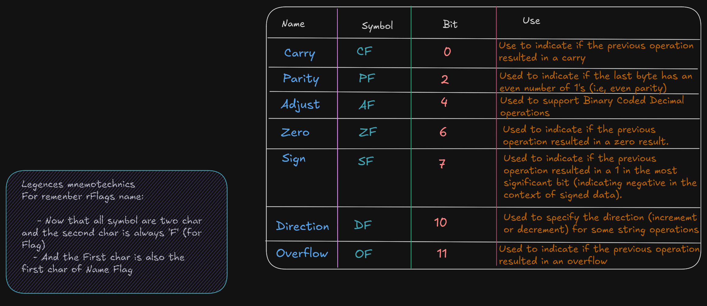
Flag Register (rFlags)
A flag register, rFlags is used for store status and CPU control information about the instruction that
was just executed.
The rFlag is directly updated (Status) by processor and not accessible by program,
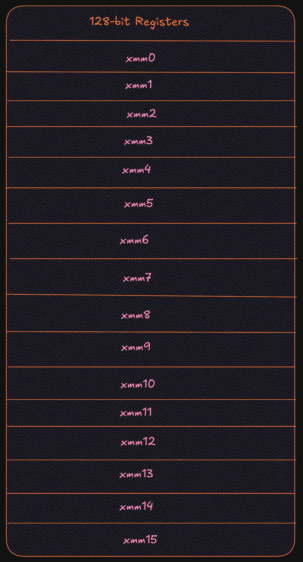
XMM registers
The XMM are set of dedicated registers used to support 32-bit and 64-bit floating point
operations and Single Instruction Multiple Data (SIMD) instructions.
SIMD allow a single instructions allow a single instruction to be applied
simultaneaously to to multiple data items, it help to increase a performance.
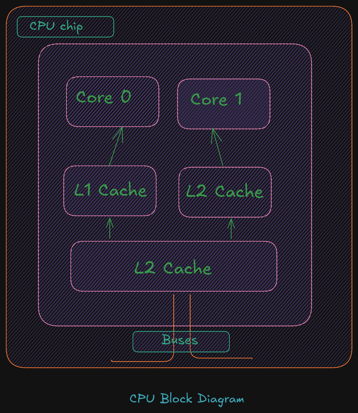
Cache Memory
Cache memory is a small subset of the primary storage or RAM located in the
CPU chip. If a memory location is accessed, a copy of the value is placed
in the cache*.
A memory read involves sending the address via the bus to the memory controller,
which will obtain the value at the requested memory location, and send it back
through the bus. Comparatively, if a value is in cache, it would be much faster
to access that value.
A cache hit occurs when the requested data can be found in a cache, while a cache miss
occurs when it cannot. Cache hits are served by reading data from the cache, which is
faster than reading from main memory. The more requests that can be served from
cache, the faster the system will typically perform.
Main memory
Memory can be viewed as a series of bytes, one after another. That is, memory is byte
addressable. This means each memory address holds one byte of information. To store
a double-word, four bytes are required which use four memory addresses.
Additionally, architecture is little-endian. This means that the Least Significant Byte
(LSB) is stored in the lowest memory address. The Most Significant Byte (MSB) is
stored in the highest memory location.

For example, assuming the value of, 5,000,000 (10) -> 004C4B40 (16), is to be placed in a
double-word variable named var1.
For a little-endian architecture, the memory picture would be as follows:
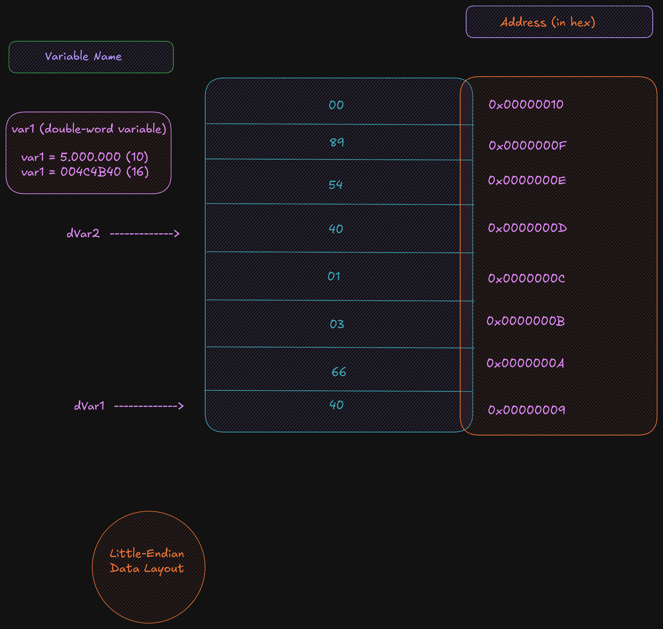
Based on the little-endian architecture, the LSB is stored in the lowest memory address
and the MSB is stored in the highest memory location.
2.5 Memory Layout
The general memory layout for a program is as shown:
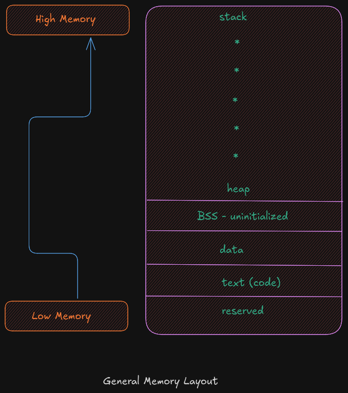
The reserved section is not available to user programs. The text (or code) section is
where the machine language (i.e., the 1’s and 0’s that represent the code) is stored. The
data section is where the initialized data is stored. This includes declared variables that
have been provided an initial value at assemble-time. The uninitialized data section,
typically called BSS section, is where declared variables that have not been provided an
initial value are stored. If accessed before being set, the value will not be meaningful.
The heap is where dynamically allocated data will be stored (if requested). The stack
starts in high memory and grows downward.
Memory Hierarchy
In order to fully understand the various different memory levels and associated usage, it
is useful to review the memory hierarchy. In general terms, faster memory is more
expensive and slower memory blocks are less expensive. The CPU registers are small,
fast, and expensive. Secondary storage devices such as disk drives and Solid State
Drives (SSD’s) are larger, slower, and less expensive. The overall goal is to balance
performance with cost.
An overview of the memory hierarchy is as follows:
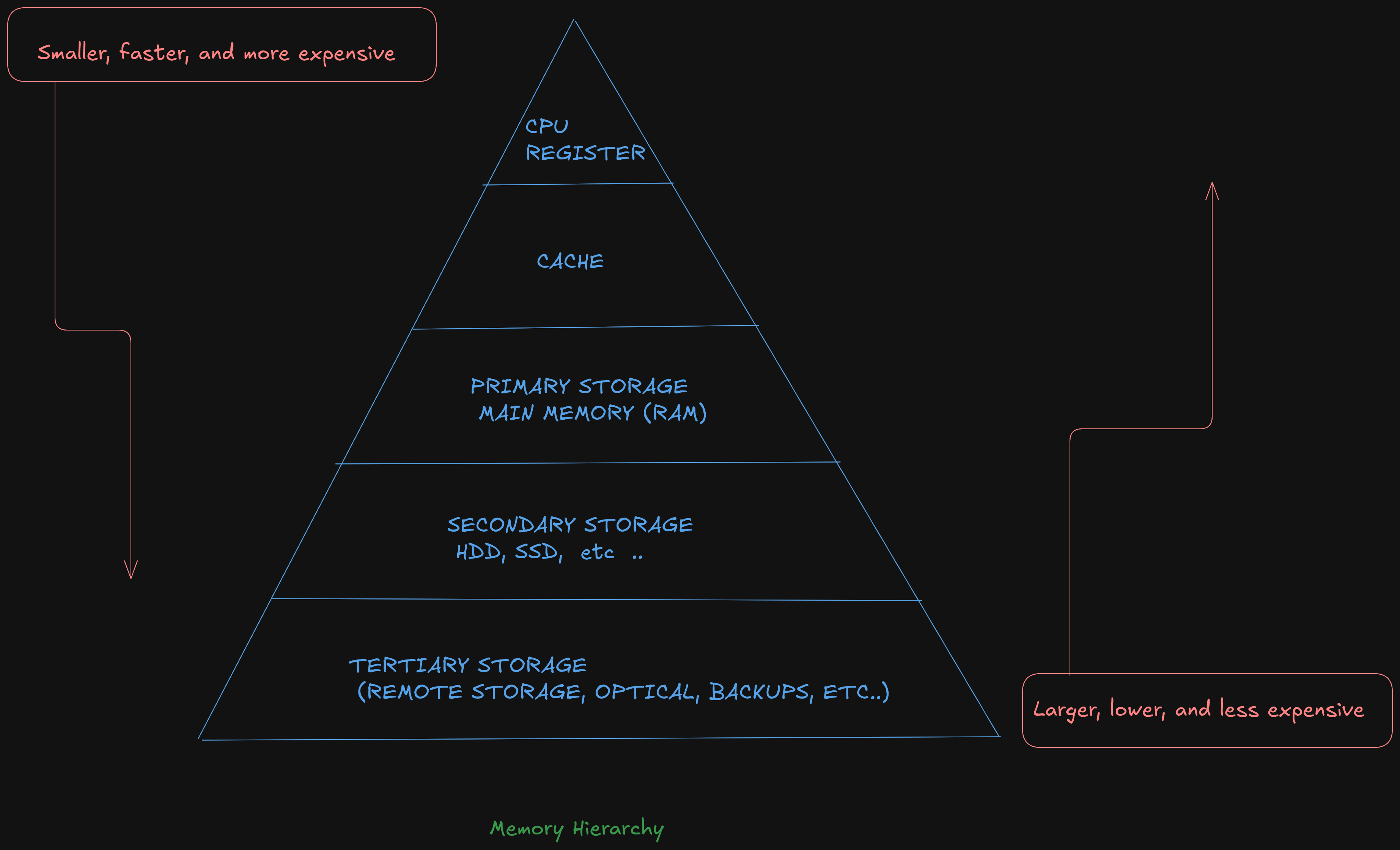
Where the top of the triangle represents the fastest, smallest, and most expensive memory. As we move down levels, the memory becomes slower, larger, and less expensive. The goal is to use an effective balance between the small, fast, expensive memory and the large, slower, and cheaper memory.
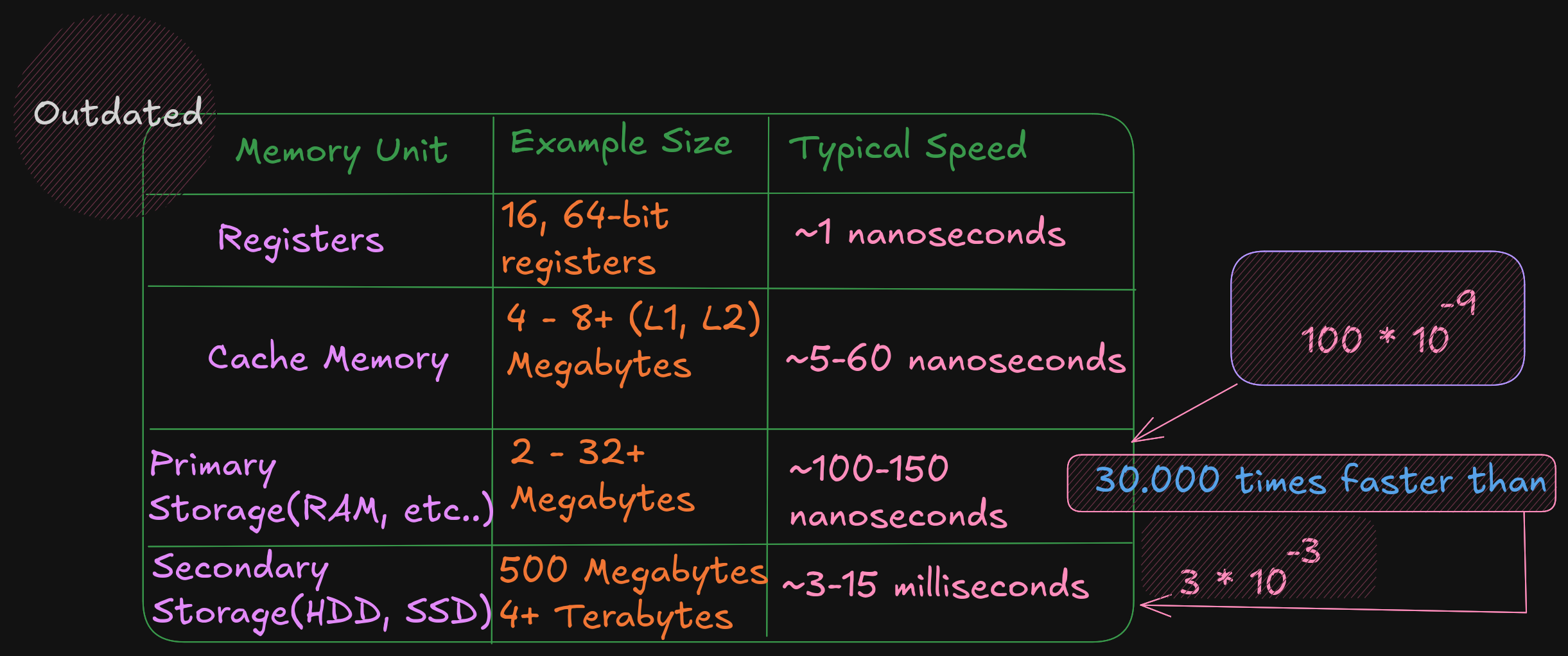
Based on this table, a primary storage access at 100 nanoseconds is 30,000 times faster than a secondary storage access, at 3 milliseconds . The typical speeds improve over time (and these are already out of date). The key point is the relative difference between each memory unit is significant. This difference between the memory units applies even as newer, faster SSDs are being utilized.